

How Does CVD Silicon Carbide Coating Solve the Inner-Wall Challenge for Hollow Lift Pins in Semiconductor Applications?
2026-09-08
1. Why Is Inner-Wall Coating the Most Critical Factor for Hollow Lift Pin Reliability?
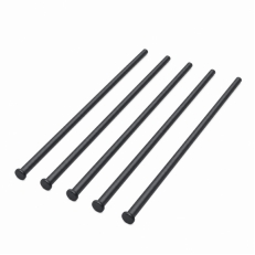
The hollow lift pin is a precision wafer handling component used inside semiconductor process equipment. Its primary function is to lift and position wafers during loading, unloading, and process sequences. Unlike conventional solid lift pins, the hollow design incorporates an internal cavity that reduces thermal mass and minimizes local heat loss. This reduction in thermal mass is critical for achieving uniform wafer temperature distribution during high-temperature processes such as epitaxial growth or annealing. However, the hollow design introduces a significant manufacturing challenge: both the inner and outer surfaces must be protected by a dense Silicon Carbide Coating. If the inner wall is left unprotected, the porous graphite substrate will release carbon particles and metallic impurities at high temperatures. Once these impurities detach, they cause color difference and particle defects on the wafer surface, severely lowering production yield. In our factory, we have evaluated lift pins from multiple suppliers and found that inner-wall coating quality is the single most important differentiator between a reliable component and one that causes yield loss.
Core challenge: The inner surface is difficult to access during the CVD coating process. Compared with the outer surface, the internal geometry introduces additional challenges in gas flow, deposition uniformity, coating thickness control, and process consistency. Therefore, inner-wall coating quality has become an important differentiating factor among suppliers.
The AMAT 0200-03201 hollow lift pin, designed for 300mm silicon epitaxy applications, exemplifies these requirements. The component must maintain precise dimensional accuracy of both inner and outer surfaces, with concentricity between the inner and outer geometries being particularly critical. Both material selection and coating processes are essential to the final performance of the lift pin. WuYi TianYao New Material Tech.Co.,Ltd. has developed a complete inner-wall coating process solution that ensures consistent coating thickness from the port to the deep interior of the bore, firm bonding, and internal bore cleanliness that meets standards.
2. What Are the Three Core Challenges of Inner-Wall Silicon Carbide Coating?
Based on our experience developing inner-wall coating processes for AMAT hollow lift pins, three technical challenges consistently emerge. The first is uncontrolled deposition uniformity. Hollow structures have a large aspect ratio. CVD reactant gases struggle to diffuse uniformly deep into the internal bore, causing the inner-wall coating thickness to decrease in a gradient from the port to the deep interior, with local areas even showing bare exposed regions. The second challenge is insufficient interfacial bonding strength. The curved inner-wall surface limits the optimization space of deposition process parameters. The bonding strength between the Silicon Carbide Coating and the graphite substrate is difficult to reach the same level as the outer surface, and micro-cracks or even peeling can easily occur during thermal cycling. The third challenge is uncontrolled internal bore cleanliness. If the porous structure of the graphite substrate is not completely sealed by the coating, carbon particles and metallic impurities will be released at high temperatures. The table below summarizes these challenges and their impact on wafer yield.
| Challenge | Root cause | Impact on yield | Conventional solution limitation |
| Non-uniform deposition thickness | Limited gas diffusion into high-aspect-ratio hollow cavity | Exposed graphite causes particle contamination | Standard CVD process optimized for outer surfaces only |
| Insufficient interfacial bonding | Curved geometry limits process parameter optimization | Coating peeling generates micro-particles | No dedicated inner-wall deposition parameter set |
| Internal bore cleanliness | Porous graphite not fully sealed by coating | Carbon particles cause color difference and defects | Incomplete sealing of inner-wall structure |
To overcome these challenges, WuYi TianYao New Material Tech.Co.,Ltd. has established a complete technical approach that integrates gas flow field simulation optimization with precise deposition temperature field control. Our Silicon Carbide Coating process is specifically designed for hollow structures, addressing each of these challenges at the process design stage.
3. How Is Inner-Wall Coating Uniformity Achieved on Hollow Lift Pins?
The uniformity of the inner-wall Silicon Carbide Coating is achieved through a combination of gas flow field simulation and precise deposition temperature field control. The process begins with the selection of a high-purity graphite substrate. Our factory typically uses imported semiconductor-grade graphite materials, including materials from SGL Carbon and Toyo Tanso, depending on customer requirements. The graphite blank undergoes precision CNC machining to achieve the required hollow geometry, with special attention paid to inner diameter, outer diameter, wall thickness, length, and concentricity. The machined graphite component then undergoes surface preparation before the CVD coating process. The critical step is the CVD Silicon Carbide Coating deposition, where the gas flow is optimized to ensure uniform diffusion into the hollow cavity. The deposition temperature field is controlled to maintain consistent coating growth on all surfaces, including the inner wall. The table below shows the key specifications of the Silicon Carbide Coating on AMAT hollow lift pins.
| Parameter | Standard specification | Verification method |
| Coating thickness | 100 ± 20 μm | Cross-section SEM |
| Coating purity | 6N (99.99995%) | GDMS analysis |
| Coating density | > 99.9% | Archimedes method |
| Surface roughness (Ra) | 0.4 – 0.8 μm | Profilometer |
| Inner-wall coverage | Full uniform coverage | Borescope + SEM |
| Thermal conductivity | 150 – 200 W/mK | Laser flash method |
The result is a Silicon Carbide Coating that provides complete protection for the graphite substrate, with the inner wall sealed as effectively as the outer surface. This is the key differentiating capability for hollow lift pins, as it ensures the internal graphite is not exposed to the high-temperature, chemically active process environment.
4. What Are the Key Manufacturing Control Nodes for Coated Hollow Lift Pins?
The production of AMAT hollow lift pins with CVD Silicon Carbide Coating involves multiple critical control nodes. The first is graphite material selection, where the appropriate high-purity graphite grade is chosen based on dimensional, thermal performance, and purity requirements. The second is precision CNC machining, where the graphite blank is machined into the required hollow geometry. The third is surface preparation, where the machined graphite component undergoes cleaning and preparation before coating. The fourth is the CVD Silicon Carbide Coating deposition itself, with special attention to the inner wall. The fifth is final inspection, where finished components undergo dimensional accuracy verification, coating condition inspection, and other customer-specified requirements. In our factory, we maintain a complete quality control system that monitors each of these control nodes.
Frequently Asked Questions About CVD Silicon Carbide Coating for Hollow Lift Pins
Summary for Semiconductor Process Engineers
The inner-wall coating of hollow lift pins is a specialized capability that directly impacts wafer yield and equipment reliability. A uniform, high-purity CVD Silicon Carbide Coating on both the outer and inner surfaces ensures that the graphite substrate is fully sealed, preventing particle contamination and maintaining purity in high-temperature process environments. The technology addresses the fundamental challenges of deposition uniformity, interfacial bonding, and internal bore cleanliness that have historically limited the performance of hollow lift pins. Our factory has developed the process controls and quality systems needed to deliver this capability consistently.
