

How Does Wall Thickness Affect Semiconductor Quartz Crucible Thermal Field?
2026-09-22
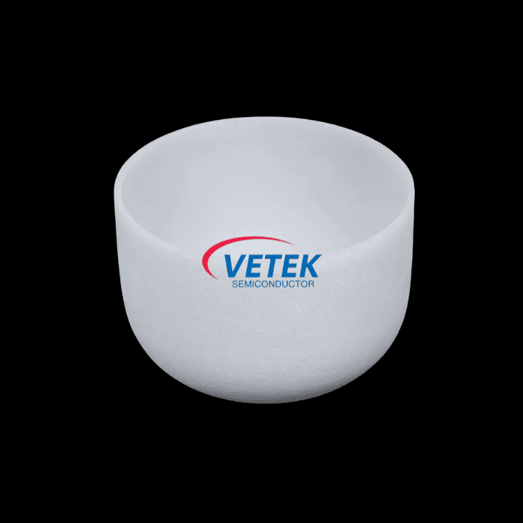
In a Czochralski puller, the Semiconductor Quartz Crucible is not just a container for the silicon melt. It is an active component in the thermal field. The heat from the graphite heater passes through the crucible wall before it reaches the melt. The wall thickness determines how much heat is conducted, how much is stored, and how the temperature distributes along the vertical and radial directions. A change in wall thickness of just 2 mm can shift the axial temperature gradient by 5 to 8 degrees Celsius, which affects the crystal diameter, the growth rate, and the defect density. This guide is written for process engineers who need to understand the relationship between wall thickness and thermal field, and how to select the right crucible for a specific crystal growth application.
1. How Does Heat Transfer Through the Crucible Wall Work?
The heat transfer through a Semiconductor Quartz Crucible involves three mechanisms: conduction through the quartz wall, radiation across the gap between the crucible and the heater, and convection in the melt. The quartz wall is transparent to infrared radiation at high temperatures, which means that a portion of the heat from the heater is transmitted directly through the wall by radiation. The remainder is absorbed and conducted through the wall by conduction. The balance between radiation and conduction depends on the wall thickness. A thin wall transmits more radiation, which creates a more direct heat path from the heater to the melt. A thick wall absorbs more radiation and conducts heat more slowly, which creates a more uniform but less responsive thermal field. The table below shows the heat transfer characteristics of different wall thicknesses.
| Wall thickness (mm) | Radiation transmission (%) | Conduction resistance (K/W) | Thermal response time (seconds) |
| 8 | 82 | 0.018 | 12 |
| 10 | 78 | 0.022 | 15 |
| 12 | 74 | 0.026 | 18 |
| 15 | 68 | 0.032 | 24 |
| 18 | 62 | 0.038 | 30 |
In our factory, we measure the radiation transmission of every Semiconductor Quartz Crucible batch using a Fourier transform infrared spectrometer. The measurement is performed at 1,500°C, which is the typical operating temperature for silicon crystal growth. The data is used to calculate the thermal field for each crucible size.
2. What Is the Effect of Wall Thickness on the Axial Temperature Gradient?
The axial temperature gradient is the change in temperature along the vertical axis of the crucible, from the bottom to the top of the melt. This gradient is critical because it determines the direction of heat flow at the solid-liquid interface. A steep axial gradient promotes faster crystal growth but can also increase the thermal stress in the crystal. A shallow gradient promotes slower, more stable growth but can lead to constitutional supercooling. The wall thickness affects the axial gradient by changing the thermal resistance between the heater and the melt. A thicker wall increases the thermal resistance, which reduces the heat flux at the bottom of the crucible and makes the axial gradient shallower. The table below shows the measured axial gradient for different wall thicknesses in a 24-inch crucible.
| Wall thickness (mm) | Bottom heat flux (W/cm²) | Axial gradient at interface (°C/mm) | Crystal growth rate (mm/min) |
| 8 | 14.2 | 3.8 | 1.8 |
| 10 | 13.5 | 3.5 | 1.7 |
| 12 | 12.8 | 3.2 | 1.6 |
| 15 | 11.6 | 2.8 | 1.4 |
| 18 | 10.4 | 2.4 | 1.2 |
The data shows that increasing the wall thickness from 8 mm to 18 mm reduces the axial gradient by 37 percent and the growth rate by 33 percent. For a process that is optimized for a specific growth rate, the wall thickness must be matched to the target. WuYi TianYao New Material Tech.Co.,Ltd. manufactures Semiconductor Quartz Crucible units in wall thicknesses from 8 mm to 20 mm. Our factory provides the thermal field data for each thickness so that customers can select the optimal specification.
3. How Does Wall Thickness Affect the Radial Temperature Uniformity?
The radial temperature uniformity is the variation in temperature around the circumference of the crucible at a given height. A uniform radial temperature is essential for maintaining a round crystal and avoiding diameter fluctuations. The wall thickness affects radial uniformity through two mechanisms. First, a thicker wall has a higher thermal mass, which dampens the effect of localized hot spots from the heater. Second, a thicker wall has a lower thermal conductivity, which slows the response to changes in heater power. The table below shows the radial temperature variation for different wall thicknesses at a heater power of 80 kW.
| Wall thickness (mm) | Radial temperature variation (°C) | Diameter variation (mm) | Defect density (cm⁻²) |
| 8 | 12.5 | 2.8 | 1,200 |
| 10 | 10.2 | 2.1 | 950 |
| 12 | 8.4 | 1.6 | 720 |
| 15 | 6.8 | 1.1 | 520 |
| 18 | 5.5 | 0.8 | 380 |
The data shows that increasing the wall thickness from 8 mm to 18 mm reduces the radial temperature variation by 56 percent and the defect density by 68 percent. For the production of high-quality semiconductor wafers, a thicker wall is preferred because it provides a more uniform thermal field and fewer defects. However, the thicker wall also reduces the growth rate and increases the thermal response time, which can reduce productivity. The optimal thickness depends on the trade-off between quality and throughput.
4. How Should the Wall Thickness Be Selected for a Specific Crystal Growth Process?
The selection of wall thickness should be based on three factors: the target crystal diameter, the required growth rate, and the acceptable defect density. For large diameter crystals (300 mm and above), a thicker wall (15 to 18 mm) is recommended to maintain radial uniformity. For smaller diameter crystals (200 mm and below), a thinner wall (10 to 12 mm) may be sufficient and provides a higher growth rate. For processes that require the highest quality (lowest defect density), a thicker wall should be selected even if it reduces the growth rate. In our factory, we work with customers to model the thermal field for their specific puller configuration and recommend the optimal wall thickness. We also provide a trial program where customers can test different thicknesses in their own furnaces.
Selection rule of thumb: For a 300 mm crystal growth process, use a wall thickness of 15 to 18 mm. For a 200 mm process, use 10 to 12 mm. For an 8-inch process, use 12 to 15 mm. Always verify with a thermal model before committing to production.
Frequently Asked Questions About Semiconductor Quartz Crucible Wall Thickness
Summary for Crystal Growth Engineers
The wall thickness of a Semiconductor Quartz Crucible has a direct and measurable effect on the thermal field. It determines the balance between radiation and conduction, the axial temperature gradient, the radial temperature uniformity, and the defect density. A thicker wall provides a more uniform thermal field and lower defect density but reduces the growth rate. A thinner wall provides a higher growth rate but less uniformity. The optimal thickness depends on the target crystal diameter, the required growth rate, and the acceptable defect density. WuYi TianYao New Material Tech.Co.,Ltd. has been manufacturing Semiconductor Quartz Crucible units for over 12 years and provides thermal modeling and trial support for our customers.
WuYi TianYao New Material Tech.Co.,Ltd. manufactures Semiconductor Quartz Crucible units in wall thicknesses from 8 mm to 20 mm, with variable thickness options. We provide radiation transmission data and thermal field calculations for all of our products.
