

How Does Water-Guided Laser Technology Enable Precision Micro-Hole Drilling in Silicon Carbide Ceramics?
2026-09-08
When a Korean semiconductor research team needed five 35mm diameter × 2mm thick N-type 4H-Silicon Carbide Ceramics substrates with Φ0.15mm through-holes, they faced a familiar problem: mechanical drilling breaks tools on hard-brittle SiC, and conventional laser drilling produces tapered holes with heat-affected zones that compromise material integrity. The project required a solution that could deliver uniform cylindrical holes from inlet to outlet, verified by SEM, with no measurable taper. This article documents how water-guided laser technology met that specification and what it means for the broader field of Silicon Carbide Ceramics micro-machining.
1. What Makes Silicon Carbide Ceramics Difficult to Machine With Conventional Methods?
Silicon Carbide Ceramics are classified as hard-brittle materials with a Vickers hardness exceeding 2500 HV and a fracture toughness of only 3 to 4 MPa·m². These properties make them ideal for semiconductor applications—high thermal conductivity, excellent chemical resistance, and a coefficient of thermal expansion matched to silicon—but they also make them notoriously difficult to machine. Mechanical drilling of Φ0.15mm holes in 2mm thick Silicon Carbide Ceramics is impractical. Tungsten carbide micro-drills break almost immediately due to the high cutting forces. Electrical discharge machining (EDM) is limited to conductive materials and is slow. Conventional laser drilling, using a focused beam in air, creates a conical taper because the beam diverges. The entrance diameter may be Φ0.15mm, but the exit diameter shrinks to Φ0.10mm or smaller, and the heat-affected zone (HAZ) can extend 50 to 100 microns into the material.
In our factory, we have evaluated all of these methods for processing Silicon Carbide Ceramics. The conclusion is consistent: for high-aspect-ratio micro-holes (depth-to-diameter ratios exceeding 10:1), none of the conventional techniques deliver acceptable results without significant post-processing. The 2mm thickness with a Φ0.15mm hole represents a 13:1 aspect ratio—well beyond the capability of standard laser drilling.
2. How Does Water-Guided Laser Technology Address the Taper Challenge in Silicon Carbide Ceramics?
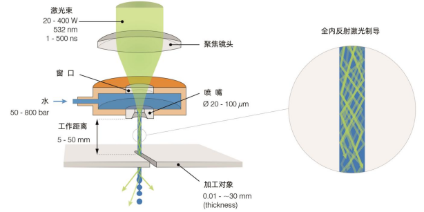
The water-guided laser method fundamentally changes how the laser energy is delivered to the workpiece. In conventional laser drilling, the beam travels through air and diverges due to diffraction. The focal point is positioned at the workpiece surface, and the energy density drops rapidly with depth. In water-guided laser technology, a high-pressure water jet (30 to 120 µm diameter) is ejected from a precision nozzle. The focused 532 nm laser beam is coupled into this water column through a glass window. Once inside the water, the laser is confined by total internal reflection, creating a parallel energy beam that propagates without divergence over a working distance of up to several tens of millimeters.
Key principle: The water jet acts as a liquid optical fiber. The laser energy remains collimated, so the cutting diameter is constant from the point of entry to the point of exit. This eliminates the taper that is inherent in free-space laser drilling. The water jet also provides continuous cooling, which suppresses the formation of a heat-affected zone on the Silicon Carbide Ceramics.
The parallel energy distribution is the reason why a one-pass through-hole is possible in 2mm thick Silicon Carbide Ceramics. The process requires no focus tracking because the beam does not diverge. The entrance and exit diameters are essentially equal, with an inlet-to-outlet difference of only 10 to 20 microns. In the recent project, the Φ0.15mm holes were confirmed by SEM to be uniform from the laser-entry side to the exit side, meeting the customer's stringent requirements for secondary-battery material development.
3. What Processing Parameters Enable Taper-Free Φ0.15mm Holes in 2mm Silicon Carbide Ceramics?
The successful processing of Φ0.15mm holes in 2mm thick Silicon Carbide Ceramics depends on a set of precisely controlled parameters. The table below shows the key parameters from the recent project, along with their significance.
| Parameter | Value used in project | Significance for Silicon Carbide Ceramics |
| Laser wavelength | 532 nm | Green laser provides higher absorption in SiC than IR wavelengths |
| Laser power | 50 – 60 W | Sufficient for ablation of 2mm thickness in single pass |
| Water jet diameter | 30 – 120 µm | Determines the kerf width; 30µm jet for fine holes |
| Water pressure | 300 – 500 bar | Maintains stable jet and provides cooling; force at workpiece ~1N |
| Feed rate | 100 – 300 mm/min | Optimized for surface quality and throughput |
| Working distance | Up to 60 mm | Beam remains collimated over full thickness |
| Measured outcome | Result for Silicon Carbide Ceramics | Acceptance criterion |
| Hole diameter (inlet) | Φ0.15mm | ±0.01mm |
| Hole diameter (exit) | Φ0.13 – 0.15mm | No measurable taper |
| Surface roughness (Ra) | 0.3 – 1.0 µm | ≤ 1.5 µm |
| Heat-affected zone | Minimal, not measurable | No recast layer |
| Aspect ratio | 13:1 (2mm / 0.15mm) | Exceeds 10:1 target |
WuYi TianYao New Material Tech.Co.,Ltd. has validated these parameters on our WL-DCS200 equipment platform. The 50-60W power level and 532nm wavelength are the standard configuration for processing Silicon Carbide Ceramics. We also offer the WL-LCS500 platform with 100-200W power for larger work areas up to 500×500 mm.
4. What Does SEM Verification Reveal About Hole Quality in Silicon Carbide Ceramics?
The project deliverable included SEM imaging of the hole cross-sections. The images confirmed three critical attributes. First, the hole geometry was cylindrical and uniform from the inlet to the outlet. No taper was visible within the SEM measurement resolution, which is consistent with the parallel energy beam principle. Second, the hole walls were smooth, with a surface roughness within the Ra 0.3 to 1.0 µm specification. Third, there was no observable heat-affected zone, no recast layer, and no chipping at the edges. The continuous water flow during processing cools the SiC and flushes the debris before it can redeposit.
Project outcome: The customer accepted all five 35mm diameter × 2mm thick Silicon Carbide Ceramics substrates. The parts are now being evaluated in a silicon-alloy anode material development program for next-generation lithium-ion batteries. This application requires uniform, defect-free holes to ensure consistent material properties and reliable battery performance.
Frequently Asked Questions About Water-Guided Laser Processing of Silicon Carbide Ceramics
Summary for Semiconductor Materials Engineers
The water-guided laser method provides a reliable solution for processing high-aspect-ratio micro-holes in Silicon Carbide Ceramics. The technology addresses the fundamental limitations of conventional machining: the parallel water-jet-guided beam eliminates taper, the continuous water cooling prevents heat damage, and the one-pass capability eliminates alignment errors. The Φ0.15mm holes in 2mm SiC substrates, verified by SEM, demonstrate the capability for semiconductor-grade applications.
WuYi TianYao New Material Tech.Co.,Ltd. provides water-guided laser processing services for Silicon Carbide Ceramics and other advanced ceramics. We offer technical consultation, process development, and full inspection reporting. Our engineering team can assist with custom substrate preparation, including coatings and precision machining.
